Material Synthesis
Developing advanced nanomaterials, including graphene and carbon nanotubes, for emerging technologies.
Advanced materials and device innovation — bringing research, characterization and next-generation applications together on one platform.
From material development to device validation, explore the capabilities supporting nanoelectronics research and innovation.
Developing advanced nanomaterials, including graphene and carbon nanotubes, for emerging technologies.
Precision fabrication and assembly processes for innovative nanoelectronic devices.
Simulation, characterization and validation to evaluate device design and performance.
Research and device imagery highlighting work developed using ion-beam techniques at the IC IIT Patna Lab, supported by ACNN, AKU.

Developed via ion beam at IC IIT Patna Lab. Supported by ACNN, AKU.


Current prototype work on YAB LEDs, doped device variants, and quantum dots.
Development of doped YAB LED using transition-metal and rare-earth dopants.
Prototype development of YAB quantum dots as part of ongoing nanoelectronics research.
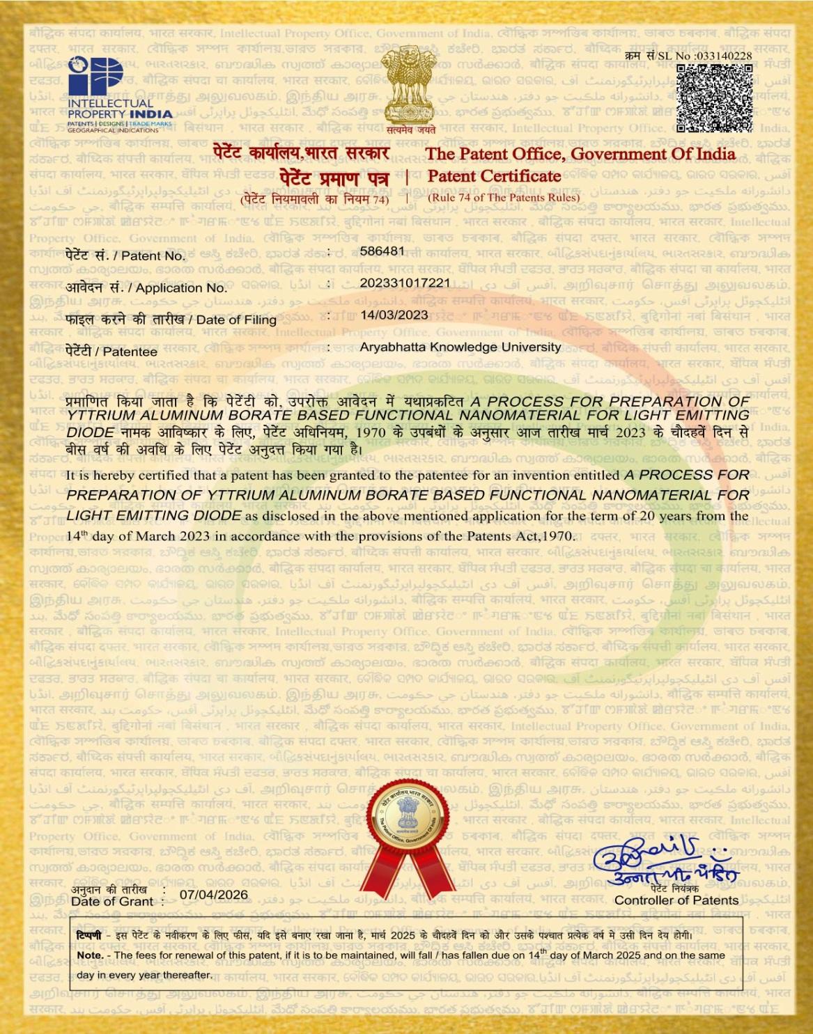
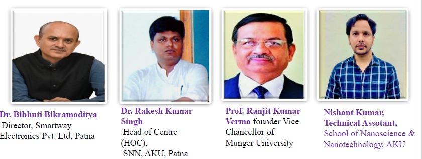
Patent information and research summary for the reported Yttrium Aluminum Borate (YAB) nanomaterial.
An economical method for preparing highly efficient Yttrium Aluminum Borate (YAB) nanomaterial with photoluminescence across the ultraviolet and visible range (400–451 nm), described as suitable for high-index LEDs and as non-hazardous to humans and animals.
We are a startup company @ Incubation Center, IIT Patna working in the field of Medical Electronics, Embedded system, Micro-electronics, Nano electronics, Internet of Things (IoT) and Robotics and system software related Research & Development, product prototyping and Design servicing. It has been established with an aim to develop center of advanced electronics research & development At SMARTWAY ELECTRONICS, we take pride in design innovation and accept engineering challenges for developing quality products.
Patna Office: Malti Niwas, Road No-1, Dhelwan, Near Bus Stand Bypass Road, Patna-13, Pin: 800030,
Email: smartwayelectronics20@gmail.com, Mob: +91-6299818933
View on Map
Bangalore Office: Bangalore Bioinnovation Centre BS09, Ground Floor, Bangalore Helix Biotech Park, BBC, Electronic City Phase-1, Bangalore- 560100, Mob: +91-8002359537
Mumbai Office: Plot No.177, Shree Niwas, B-301, Sector 14, Nerul (west), Navi Mumbai– 400706, Mob: +91-8108475077


© copyright 2025: Smartway Electronics